Introduction
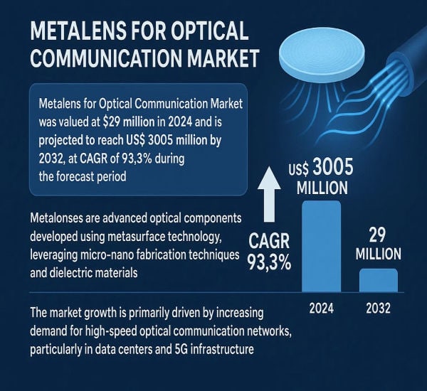
The Metalens for Optical Communication Market was valued at USD 29 million in 2024 and is forecast to surge to USD 3,005 million by 2032, reflecting a blistering CAGR of 93.3% through the period. This dramatic expansion is driven by needs for higher bandwidth, smaller form factors and improved energy efficiency in next-generation networks.
𝐃𝐨𝐰𝐧𝐥𝐨𝐚𝐝 𝐅𝐑𝐄𝐄 𝐒𝐚𝐦𝐩𝐥𝐞 𝐑𝐞𝐩𝐨𝐫𝐭: https://semiconductorinsight.com/download-sample-report/?product_id=117839
Emerging Trends Shaping the Market
Computation-Designed Metasurfaces and AI-Optimized Optics
AI-driven design tools accelerate development of metalenses by optimizing nanostructure geometry for broadband, achromatic performance. These computational approaches shorten prototyping cycles and enable metalenses tailored to dense WDM and chip-scale interconnect applications.
Wafer-Scale Nanofabrication & Advanced Lithography
Advances in nanoimprint lithography and high-resolution patterning are moving metalenses from lab demonstrations toward mass production. Wafer-scale processes and imprint technologies from firms like NILT promise the reproducibility and cost reductions necessary for telecom deployment.
Rise of Compound Materials and Silicon Photonics Integration
Integration with silicon photonics and use of compound substrates such as GaAs and TiO₂ enable metalenses to meet performance targets across infrared and visible bands. This materials convergence supports deployments in data centers, 5G fronthaul and free-space optical links.
Miniaturization and System-Level Consolidation
Metalenses replace multi-element optics with single planar surfaces, shrinking transceiver footprints by an estimated 30–40% and simplifying mechanical assemblies—critical for small-cell and edge installations where space and power are constrained.
Key Market Drivers and Growth Factors
- Exploding data demand: Global internet traffic and hyperscale AI workloads are driving investment in higher-capacity optical interconnects.
- Footprint reduction priorities: Telecom and data center OEMs favor compact, energy-efficient modules where metalenses deliver tangible size and cost advantages.
- Performance at scale: Demonstrated transmission efficiencies approaching 90% and multi-wavelength operation lower system loss and improve signal integrity.
- Manufacturability advances: Nanoimprint and semiconductor-foundry partnerships enable wafer-scale production and lower per-unit costs.
- Strategic infrastructure projects: 5G densification, edge compute rollouts and hyperscale optical upgrades create sizeable addressable markets.
𝐆𝐞𝐭 𝐅𝐮𝐥𝐥 𝐑𝐞𝐩𝐨𝐫𝐭 𝐇𝐞𝐫𝐞: https://semiconductorinsight.com/report/metalens-for-optical-communication-market/
Strategic Developments by Key Players
- Shenzhen Metalenx Technology Co., Ltd: Scaling infrared metalens production for fiber-optic transceivers and strengthening Asia-Pacific distribution.
- NIL Technology (NILT): Pushing nanoimprint lithography solutions to enable wafer-scale replication and reduce fabrication costs.
- Moxtek: Expanding polarization and metasurface product lines aimed at free-space optical and sensing markets.
- Hangzhou Najing Technology & shphotonics: Targeting visible-light interconnects and cost-competitive manufacturing for short-reach applications.
- Strategic initiatives: Firms are pursuing vertical integration, foundry partnerships, and hybrid optical subsystems that combine conventional optics with metalens elements.
Segment Analysis: Who Leads the Market?
- By Type: Infrared metalenses dominate due to long-distance optical communication needs; visible metalenses gain traction in short-range data center links.
- By Application: Optical fiber communication is the primary revenue source, followed by sensing and free-space links.
- By Material: Silicon-based metalenses command share for chip-scale integration; GaAs and TiO₂ offer specialty performance.
- By Region: Asia-Pacific emerges fastest, propelled by telecom investment and domestic manufacturing capacity; North America and Europe retain leadership in high-value R&D and early deployments.
𝐃𝐨𝐰𝐧𝐥𝐨𝐚𝐝 𝐅𝐑𝐄𝐄 𝐒𝐚𝐦𝐩𝐥𝐞 𝐑𝐞𝐩𝐨𝐫𝐭: https://semiconductorinsight.com/download-sample-report/?product_id=117839
Technological Advancements Impacting Growth
Can Computation-Driven Nanofabrication Unlock Commercial Metalenses?
Yes,combined advances in design algorithms, imprint lithography and materials science are removing barriers to scale. Improved achromatic designs and multi-wavelength capability make metalenses viable replacements for several conventional optical assemblies, enabling higher integration density and lower system costs.
Why This Report Matters
This analysis provides actionable intelligence for equipment makers, foundries and network operators by delivering:
- Market estimates and forecasts (2024–2032) reflecting the extraordinary CAGR and TAM expansion.
- Competitive mapping of key technology suppliers and manufacturing pathways.
- Opportunity maps showing where commercialization, partnerships and investment will yield the greatest returns.
- Scenario-based insights linking network build-outs, AI-driven data growth and manufacturability milestones to adoption timelines.
𝐆𝐞𝐭 𝐅𝐮𝐥𝐥 𝐑𝐞𝐩𝐨𝐫𝐭 𝐇𝐞𝐫𝐞: https://semiconductorinsight.com/report/metalens-for-optical-communication-market/
Conclusion
Given the convergence of computational design, materials innovation and scalable fabrication, metalenses are positioned to disrupt optical communications across multiple layers—from chip-scale interconnects to long-haul subsystems. Stakeholders that combine manufacturing partnerships with system-level integration will be best placed to capture the rapid growth window ahead.
Contact Us:
🌐 Website: https://semiconductorinsight.com/
📞 International: +91 8087 99 2013
🔗 LinkedIn: Follow Us