Introduction
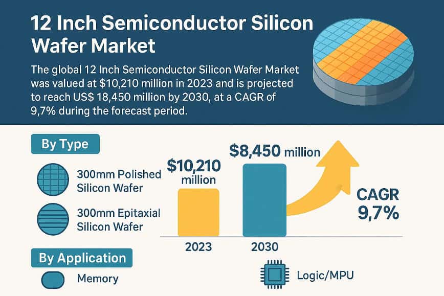
According to semiconductorinsight, the global 12-inch semiconductor silicon wafer market, valued at USD 10.21 billion in 2023, is on track to reach USD 18.45 billion by 2030, registering a 9.7% CAGR. This rapid acceleration underscores the vital role of 300mm wafers in powering next-generation chip manufacturing across AI, automotive, and consumer electronics. The semiconductor industry continues to redefine global innovation, with this market showing robust expansion and technological disruption.
Download Sample Report PDF https://semiconductorinsight.com/download-sample-report/?product_id=92885
Emerging Trends Shaping the Market
AI-Driven Automation Accelerates Wafer Production
AI-enabled production systems are improving wafer yield, defect detection, and lithography precision. As chip nodes shrink and complexity rises, 12-inch wafers benefit significantly from smarter automation that reduces cycle times and enhances operational consistency across fabs.
EUV Lithography Expands at Advanced Nodes
The shift toward 5nm, 3nm, and sub-3nm processes is driving a wider reliance on EUV lithography. This technology demands exceptionally pure and uniform 12-inch wafers, reinforcing their role as the foundation of cutting-edge device fabrication for high-performance computing and advanced logic chips.
Growing Adoption of Power Semiconductors
While silicon carbide (SiC) and gallium nitride (GaN) are on the rise, large-diameter silicon wafers remain critical for mainstream power device manufacturing. Their scalability and mature ecosystem ensure continued relevance as industries electrify—from EVs to renewable energy systems.
3D Packaging and Heterogeneous Integration
Innovations such as chiplet architectures and 3D stacking are increasing the requirement for ultra-flat, low-defect 12-inch wafers. These advanced packaging methods depend on precise substrates capable of supporting higher interconnect density and thermal stability.
Sustainability and Green Manufacturing
With fabs consuming vast amounts of energy and water, sustainability is becoming a defining trend. Manufacturers of 12-inch wafers are adopting circular processes, recycling materials, and integrating energy-efficient equipment to align with environmental standards and customer expectations.
Key Market Drivers and Growth Factors
- Rising demand for high-performance chips in AI servers, cloud infrastructure, and 5G networks.
- Rapid expansion of EV production, boosting the need for efficient power management chips.
- Global investments in logic, memory, and specialty fabs to secure supply chain resilience.
- Transition toward advanced nodes that require ultra-flat and high-purity 300mm wafers.
- Increased consumption of consumer electronics and industrial automation systems.
Strategic Developments by Key Players
Leading companies are accelerating capacity expansions, technology upgrades, and material innovations to meet unprecedented demand:
- Shin-Etsu Chemical continues to reinforce its position through high-purity wafer production and strategic investments in next-generation substrate technology.
- SUMCO is expanding 300mm wafer capacity to support advanced logic and memory fabs across Asia and North America.
- GlobalWafers has increased its global footprint through fab expansions and supply partnerships with major semiconductor manufacturers.
- Siltronic AG is advancing wafer surface engineering and nanometer-level polishing processes tailored for EUV technologies.
- SK Siltron is strengthening domestic supply chains and investing in large-diameter wafer R&D to support the fast-growing chipmaking ecosystem in South Korea.
- FST Corporation contributes to specialized wafer solutions designed for high-thermal and high-precision semiconductor applications.
Our comprehensive report is ready with the latest trends, growth opportunities, and strategic analysis https://semiconductorinsight.com/report/12-inch-semiconductor-silicon-wafer-m
Segment Analysis: Who Leads the Market?
By Application
Logic devices and advanced computing chips represent the largest share, driven by data-center demand and intensive AI workloads. Memory chips also play a significant role as cloud storage expands globally.
By Region
Asia-Pacific dominates, fueled by strong fabrication ecosystems in Taiwan, South Korea, Japan, and increasingly China. North America remains a strategic hub for advanced logic and R&D-driven manufacturing, supported by expanding government incentives.
By Technology Node
Sub-7nm processes exhibit the fastest growth, given their reliance on superior wafer flatness, uniformity, and defect-free surfaces.
Technological Advancements Impacting Growth
Can AI-Driven Lithography Redefine Semiconductor Yield Rates?
AI-assisted lithography is becoming central to reducing overlay errors and improving patterning accuracy. This advancement directly influences the value of 12-inch wafers, which serve as the preferred substrate for high-volume manufacturing at advanced nodes.
Nanofabrication breakthroughs, automation in cleanroom workflows, and smarter inspection systems are collectively shaping the next era of wafer innovation. These technologies streamline production, minimize contamination, and enhance scalability for leading foundries.
Why This Report Matters
Stakeholders evaluating the 12-inch semiconductor silicon wafer landscape gain access to:
- Market estimations through 2032
- Competitive intelligence on global wafer manufacturers
- Technological and regional opportunity assessment
- Strategic growth mapping for OEMs, material suppliers, and investors
These insights offer actionable clarity to decision-makers navigating a rapidly evolving semiconductor supply chain.
Download Sample Report PDF https://semiconductorinsight.com/download-sample-report/?product_id=92885
Forward View
As the semiconductor landscape evolves at record speed, stakeholders must align innovation with sustainability and strategic foresight to remain competitive. With 12-inch wafers at the core of next-generation chip production, their global demand is expected to strengthen significantly through the next decade.
Explore Related Outgoing Coverage in semicoductorinsight Domain
https://semiconductorinsight.com/report/gas-scrubbers-for-semiconductor-market/
https://semiconductorinsight.com/report/flip-chip-market/
https://semiconductorinsight.com/report/track-luminaires-market/
https://semiconductorinsight.com/report/ethernet-to-fiber-media-converter-market/
https://semiconductorinsight.com/report/global-polka-dot-beamsplitters-market/
https://semiconductorinsight.com/report/global-rectifiers-market/
Call-to-Action
Explore more semiconductor insights, forecasts, and technology updates at Semiconductor Insights