Introduction
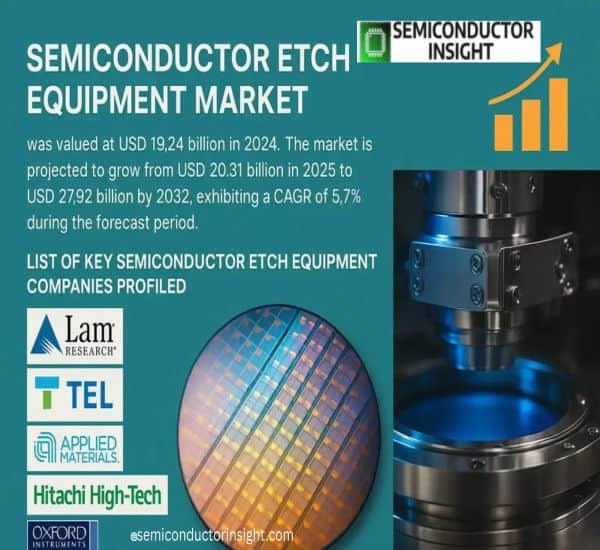
The global Semiconductor Etch Equipment Market, valued at USD 19.24 billion in 2024, is set to reach USD 27.92 billion by 2032, expanding at a 5.7% CAGR from an estimated USD 20.31 billion in 2025. The semiconductor industry continues to redefine what’s possible at the nanoscale: etch tools — which carve the circuit patterns that make modern chips work — are now central to scaling nodes, enabling three-dimensional architectures and meeting the performance demands of AI, HPC and next-generation mobile networks.
𝐃𝐨𝐰𝐧𝐥𝐨𝐚𝐝 𝐅𝐑𝐄𝐄 𝐒𝐚𝐦𝐩𝐥𝐞 𝐑𝐞𝐩𝐨𝐫𝐭: https://semiconductorinsight.com/download-sample-report/?product_id=127135
Emerging Trends Shaping the Market
Atomic-Level Control with Atomic Layer Etching (ALE)
ALE moves etching from rate-driven processes to atomic precision, enabling high-aspect-ratio features and protecting critical device layers. This capability is becoming essential for sub-5nm logic and advanced memory.
Process Integration for 3D Architectures
As 3D NAND, stacked dies and chiplet integration proliferate, etch tools must support complex patterning, via formation and selective etch steps across heterogeneous materials—driving demand for specialty chemistries and modular toolsets.
AI-Driven Process Monitoring and Predictive Maintenance
Machine learning for real-time endpoint detection and anomaly prediction is improving throughput and yield while reducing downtime. Etch platforms embedded with analytics are becoming standard in modern fabs.
Plasma Chemistry and Low-Damage Etching
New plasma sources and chemistries minimize substrate damage and improve selectivity, addressing sensitivity requirements for high-k/metal gate stacks and delicate interconnect layers.
Scale-Out Support for Emerging Wafer Sizes
While 300mm remains dominant, early development for 450mm and continued attention to 200mm process reliability keep etch vendors focused on flexible tool architectures that support multiple wafer formats.
Key Market Drivers and Growth Factors
- Advanced node transitions toward 2nm and beyond require etchers with tighter control and repeatability.
• Boom in AI and high-performance compute fuels demand for logic chips with aggressive patterning and etch complexity.
• Fab expansions in Asia-Pacific create sustained capital equipment cycles and regional service demand.
• Rise of advanced packaging and TSVs introduces back-end etch requirements beyond traditional front-end markets.
• Yield and cost pressures push fabs to adopt automation and inline metrology integrated with etch tools.
𝐆𝐞𝐭 𝐅𝐮𝐥𝐥 𝐑𝐞𝐩𝐨𝐫𝐭 𝐇𝐞𝐫𝐞: https://semiconductorinsight.com/report/semiconductor-etch-equipment-market/
Strategic Developments by Key Players
Market leaders — Lam Research, Tokyo Electron (TEL), Applied Materials, Hitachi High-Tech, Oxford Instruments and SPTS (KLA) — are accelerating R&D in ALE, advanced plasma sources and modular, serviceable tool designs. Common strategic moves include pilot tool deployments with leading foundries, regional service network expansions in Asia-Pacific, and partnerships with materials suppliers to co-develop chemistries that enhance selectivity and reduce defectivity.
Segment Analysis: Who Leads the Market?
By Type — Dry etch equipment dominates logic and memory fab volumes due to precision requirements; wet etch remains important for certain process flows and legacy nodes.
By Application — Advanced logic and memory are the largest revenue contributors; MEMS and power device fabrication present growing opportunities tied to electrification and IoT trends.
By End User — Foundries and IDMs drive capital spending for leading-edge tools; memory manufacturers create cyclical demand spikes tied to node transitions.
By Wafer Size — 300mm tools account for the bulk of current spending; flexible architectures supporting multiple wafer sizes command a premium for fabs pursuing mixed production.
𝐃𝐨𝐰𝐧𝐥𝐨𝐚𝐝 𝐅𝐑𝐄𝐄 𝐒𝐚𝐦𝐩𝐥𝐞 𝐑𝐞𝐩𝐨𝐫𝐭: https://semiconductorinsight.com/download-sample-report/?product_id=127135
Technological Advancements Impacting Growth
Can AI-enabled control tame atomic-scale variability? Combining ALE, advanced endpoint detection and machine learning is improving uniformity and throughput while reducing over-etch risk. Innovations in reactor design and materials science are also extending etch capability into new materials stacks required by GAA transistors and heterogeneous integration.
Why This Report Matters
This analysis offers:
• Market estimates and revenue forecasts (2024–2032) with node-level implications.
• Detailed segmentation by type, application, wafer size and region.
• Competitive benchmarking and supplier strategy insights.
• Technology trend mapping and opportunity identification for tool OEMs, materials suppliers and fab owners.
𝐆𝐞𝐭 𝐅𝐮𝐥𝐥 𝐑𝐞𝐩𝐨𝐫𝐭 𝐇𝐞𝐫𝐞: https://semiconductorinsight.com/report/semiconductor-etch-equipment-market/
𝐂𝐨𝐧𝐜𝐥𝐮𝐬𝐢𝐨𝐧
As semiconductor nodes shrink and packaging complexity rises, etch equipment will shift from commodity hardware to strategic enabler — the precision, integration and intelligence of etch platforms will directly influence chip performance, yield and time-to-market. Companies that invest in atomic-scale process control, service excellence and AI-assisted operations will be best positioned to capture share in this steady, technically driven market expansion.
Contact Us:
🌐 Website: https://semiconductorinsight.com/
📞 International: +91 8087 99 2013
🔗 LinkedIn: Follow Us