Key Highlights
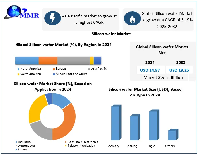
Market valuation stood at USD 14.97 billion in 2024 and is projected to scale to USD 19.25 billion by 2032, advancing at a compound annual growth rate (CAGR) of 3.19% over the 2025–2032 forecast matrix.
The 300 mm wafer dimension stands as the dominant size segment, favored by top-tier fabrication plants to systematically reduce production costs per unit area.
The memory segment commands the type classification matrix, driven by high global consumption of DRAM and NAND flash storage chips inside corporate data centers and mobile hardware.
Consumer electronics represents the dominant application framework, propelled by the high-volume manufacturing and worldwide delivery of smartphones, laptops, and connected wearables.
Severe entry barriers, high capital investment costs, strict environmental regulations, and associated environmental hazards remain primary structural constraints limiting rapid market entry.
Why This Matters Now
Semiconductor manufacturing operations face an immediate operational crisis if they fail to align substrate orders with structural shifts in size efficiency and high-purity material availability. Industrial device producers who ignore the structural migration toward advanced automated wafer architectures risk long-term volume shortfalls as global technology ecosystems shift toward specialized artificial intelligence and green energy manufacturing nodes. This manufacturing movement redefines basic foundry margin metrics, transforming low-tier substrate purchasing into a highly strategic battle for long-term component security.
Market Overview
The global silicon wafer market is undergoing a calculated infrastructure expansion, growing from an established baseline value of USD 14.97 billion in 2024 to a projected revenue target of USD 19.25 billion by 2032. This performance trajectory reflects a steady compound annual growth rate of 3.19% across the designated eight-year forecast window spanning from 2025 to 2032. The historical operational records from 2019 through 2024 confirm a permanent baseline demand for high-purity silicon substrates across key microelectronic supply loops.
This financial expansion demonstrates that enterprise capital is migrating toward hardware configurations that optimize yield efficiency per total surface area. Contemporary fabrication facilities are concentrating engineering investments on specialized ingot slicing, chemical-mechanical planarization, and cleanroom sorting arrays to supply standard substrates to global microchip design houses.
Key Trends Driving Growth
The massive adoption of smart, interconnected consumer devices and automated industrial machinery is forcing a complete restructuring of global foundry supply strategies. The primary growth driver remains the steady rollout of advanced mobile networks, automated enterprise factory lines, and high-performance computing centers that require vast volumes of integrated circuits. This structural requirement ensures a stable, recurring revenue stream for material suppliers capable of maintaining pure silicon crystal outputs under strict compliance guidelines.
Concurrently, rising household income and shifting standards of living across developing nations are elevating the long-term consumption metrics of personal technology hardware. End-users require higher processing performance, expanded onboard storage space, and rapid data speeds, which translates directly to greater substrate consumption per device manufactured. This widespread consumer technology reliance encourages tier-one semiconductor vendors to secure multi-year material contracts, preventing spot-market price spikes from breaking operational cost models.
Segment Insights
Dominant Size Segment: The 300 mm wafer segment commands the largest share of total manufacturing volume. This clear leadership proves that industrial chip builders choose to run high-volume fabrication operations using larger surface diameters to lower production costs per unit area, optimizing factory margins.
Dominant Type Segment: The Memory segment dominates the product type matrix, driven by a global surge in data usage that requires massive installations of DRAM and NAND flash modules. This continuous chip demand comes from expanded cloud computing architectures, machine learning laboratories, and consumer storage networks.
Dominant Application Segment: Consumer Electronics represents the leading application pathway, sustained by the permanent manufacturing lines dedicated to global smartphone, tablet, smart television, and wearable computing delivery.
Fastest-Growing Region: North America is positioned as a highly significant expansion corridor, experiencing an accelerated growth rate driven by the integrated deployment of silicon wafers within commercial solar cell and clean energy networks.
Alternative Size Sub-Segments: The broader market maintains active operational tracking across alternative dimensional standards, including legacy 150 mm options, mid-tier 200 mm setups, and ultra-advanced 450 mm system structures.
Regional Growth Story
The Asia Pacific region held the absolute highest market share in 2024, anchoring the global supply network for consumer electronics assembly and foundry infrastructure. The region benefits from massive concentrations of specialized microchip fabrication facilities, highly organized component ecosystems, and deep manufacturing pools in key industrial centers. This regional dominance allows local suppliers to maintain high utilization rates, setting the pricing baseline for global substrate transactions.
Concurrently, the North American marketplace is experiencing a notable growth acceleration, driven by a national push to integrate safe, clean, and reliable domestic energy alternatives across the United States and Canada. This regional energy transition relies directly on the accelerating production of high-performance photovoltaic solar cells, which utilize silicon wafers to convert solar radiation into electricity. This clean-energy framework introduces an entire secondary demand structure for silicon material processors outside traditional computing and telecommunication applications.
Competitive Landscape
The global silicon wafer sector includes prominent material engineering corporations and specialized processing companies such as Kinik Company, KST World Corp., Mimasu Semiconductor Industry Co. Ltd., MOSPEC Semiconductor Corporation, NanoSilicon, Inc., Noel Technologies, Inc., North East Silicon Technologies, Inc., and Optim Wafer Services. This highly specialized marketplace operates under intense technical demands, where chemical purity levels, flatness tolerances, and ingot quality decide market share retention. Low-tier processing plants face severe margin compression as energy costs rise and dominant leaders utilize massive vertical integration to control raw silicon crystal access.
To defend their corporate positions, established players are executing aggressive manufacturing upgrades and structured partnerships to protect long-term delivery channels to major foundries. These corporate strategic actions indicate that the next 12 to 24 months will bring portfolio realignments, with asset-heavy corporations acquiring niche wafer reclamation or processing firms to insulate supply chains from global disruption. Rivals must prepare for a market environment where basic substrate supply contracts are increasingly tied to strict environmental compliance guarantees and carbon-neutral manufacturing mandates.
Recent Developments
Material processing firms expanded capital allocations toward high-diameter wafer tools, optimizing automated production setups for 300 mm and larger substrates to capture foundry scale efficiencies.
Industrial engineering groups integrated advanced chemical-mechanical planarization methods, lowering surface defect densities to satisfy strict quality rules for next-generation logic chips.
Substrate suppliers established dedicated logistical paths to feed the expanding North American solar cell manufacturing sector, shifting product volume toward photovoltaic cell buyers.
Strategic Implications
Procurement executives and supply chain managers must immediately adjust their material-sourcing portfolios to favor long-term, index-priced contracts for 300 mm wafers over volatile spot-market purchasing. Relying on short-term merchant availability represents a severe operational risk when global data center expansions and automotive automation trends consume massive quantities of baseline memory chips. Furthermore, manufacturing groups must rapidly upgrade their factories to comply with ascending environmental standards to protect their preferred-vendor statuses with global electronics brands.
Product engineering teams must focus on minimizing cutting waste while optimizing the crystal purity profiles of their silicon ingots. High material costs and strict hazardous waste regulations mean factories must achieve near-zero defect rates during high-speed diamond-wire slicing stages. Processing plants that fail to incorporate advanced thermal monitoring and automated crystal growth systems will find themselves disqualified from major institutional supply agreements.
Future Outlook
The market will separate into highly profitable material engineering groups that control large-diameter premium fabrication lines and certified clean-energy supply agreements, and undifferentiated commodity wafer processors whose margins will be crushed by strict international environmental penalties and high capital entry costs.
Analyst Perspective
“The rapid modernization of the global silicon wafer market highlights a permanent structural transition toward large-diameter efficiency and clean-energy application loops,” states Rucha Deshpande, Research Analyst. “As international technology groups scale up their data center footprints and regional solar installations expand, those material processing enterprises that successfully pair automated high-purity production lines with secure, traceable supply chains will capture dominant market shares across both the mature Asia Pacific foundry networks and the fast-growing North American renewable sector.”
About Maximize Market Research
Maximize Market Research Pvt. Ltd. (MMR) is a global market research and consulting company that provides reliable, data-focused, and practical business insights. The firm serves a wide range of industries, including healthcare, pharmaceuticals, technology, automotive, electronics, chemicals, personal care, and consumer goods. Through market forecasts, competitive analysis, strategic consulting, and industry impact assessments, MMR helps organizations understand changing market conditions, identify growth opportunities, and make informed business decisions for long-term success.
2nd Floor, Navale IT Park Phase 3
Pune Banglore Highway, Narhe
Pune, Maharashtra 411041, India
+91 9607365656
sales@maximizemarketresearch.com
