Key Highlights
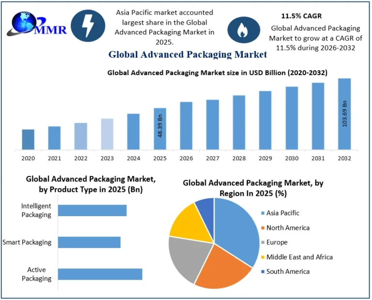
- Market valued at USD 48.39 Billion in 2025.
- Expected to reach USD 103.69 Billion by 2032.
- CAGR projected at 11.5% during 2026–2032.
- Asia Pacific remains the largest semiconductor packaging hub.
- Flip Chip technology is the leading packaging type.
- Consumer Electronics dominates end-user demand.
- AI, IoT, high-performance computing, and automotive electronics accelerate adoption.
- Miniaturization and heterogeneous integration continue reshaping semiconductor design.
- Fan-Out Wafer Level Packaging and System-in-Package technologies gain commercial traction.
- Major manufacturers continue investing in advanced packaging capacity expansion.
Why This Matters Now
Semiconductor innovation increasingly depends on advanced packaging rather than transistor scaling alone. Chipmakers are adopting sophisticated packaging architectures to improve computing performance, reduce power consumption, and integrate multiple chips into compact devices. As AI, cloud computing, automotive electronics, and next-generation consumer devices expand, advanced packaging has become a strategic differentiator across the semiconductor value chain.
Market Overview
The Advanced Packaging Market was valued at USD 48.39 billion in 2025 and is expected to reach USD 103.69 billion by 2032, expanding at a CAGR of 11.5%.
Advanced packaging combines multiple semiconductor components into highly integrated systems using technologies including 3D IC, 2.5D IC, Flip Chip, Fan-Out Wafer Level Packaging (FOWLP), Wafer Level Chip Scale Packaging (WLCSP), and System-in-Package (SiP). These technologies improve chip density, thermal performance, bandwidth, and power efficiency while enabling smaller device footprints.
Demand continues to rise as semiconductor manufacturers develop increasingly complex processors for artificial intelligence, data centers, autonomous vehicles, industrial automation, healthcare equipment, and advanced consumer electronics. Traditional packaging methods can no longer meet modern performance requirements, driving industry-wide migration toward advanced packaging solutions.
Key Trends Driving Growth
Semiconductor Miniaturization Accelerates Packaging Innovation
As transistor scaling becomes increasingly challenging, manufacturers are turning toward advanced packaging to improve chip performance. Multi-chip integration enables higher computing capability without relying solely on smaller process nodes.
AI and High-Performance Computing Increase Packaging Complexity
Artificial intelligence workloads require processors with higher bandwidth, faster communication, and lower latency. Advanced packaging technologies support heterogeneous integration by combining processors, memory, and specialized accelerators into a single package.
Consumer Electronics Continue Driving Volume Demand
Growing shipments of smartphones, tablets, wearable devices, gaming systems, and connected consumer electronics continue increasing demand for compact semiconductor packaging with improved thermal management and electrical performance.
Fan-Out and System-in-Package Technologies Gain Momentum
Fan-Out Wafer Level Packaging and System-in-Package solutions enable manufacturers to integrate multiple functions within limited board space. These technologies reduce package size while improving signal integrity and power efficiency.
Healthcare and Automotive Expand Adoption
Medical devices increasingly require miniaturized semiconductor solutions for wearable monitoring systems, robotic surgery, and diagnostic equipment. Automotive manufacturers are also integrating advanced semiconductor packages into ADAS, electric vehicles, infotainment systems, and autonomous driving platforms.
Cost Optimization Remains an Industry Priority
Although advanced packaging delivers superior performance, manufacturing costs remain significantly higher than conventional packaging. Suppliers continue investing in new production methods that improve manufacturing efficiency while lowering packaging costs for large-scale commercial deployment.
Explore detailed analysis, insights, and growth opportunities
Segment Insights
The Flip Chip segment is expected to remain the dominant packaging technology due to its superior input/output density, improved electrical performance, and compact footprint. These advantages make Flip Chip the preferred solution for automotive electronics, aerospace systems, AI processors, and high-performance computing applications where reliability and processing speed are critical.
Within industrial verticals, Consumer Electronics accounts for the largest market share. Rising demand for smartphones, wearable devices, tablets, gaming hardware, and connected consumer products continues driving adoption of advanced packaging technologies that enable thinner, lighter, and more power-efficient devices.
System-in-Package (SiP), Fan-Out Wafer Level Packaging, and 3D Integrated Circuit technologies are also witnessing increasing adoption as manufacturers integrate multiple semiconductor functions into single compact modules. These architectures reduce board space while improving system-level performance.
Regional Growth Story
Asia Pacific dominates the global Advanced Packaging Market due to its extensive semiconductor manufacturing ecosystem, expanding electronics production, and large-scale foundry investments. China, Taiwan, South Korea, and Japan remain the industry’s primary production centers.
China continues strengthening its domestic semiconductor capabilities through government-supported investment programs aimed at expanding integrated circuit manufacturing and reducing supply chain dependence.
Taiwan remains a global leader through the presence of advanced semiconductor foundries, while South Korea benefits from strong investments in memory chips, AI processors, and advanced packaging technologies by leading electronics manufacturers.
North America maintains strong demand through innovation in AI processors, cloud computing infrastructure, and advanced semiconductor research, while Europe continues expanding semiconductor capabilities across automotive, industrial automation, and aerospace applications.
Competitive Landscape
Competition remains highly concentrated among leading outsourced semiconductor assembly and test (OSAT) providers, integrated device manufacturers, and semiconductor foundries. Companies are expanding production capacity, strengthening technology partnerships, and investing in heterogeneous integration to support next-generation semiconductor architectures.
ASE Group, Amkor Technology, TSMC, Samsung Electronics, Intel, SPIL, IBM, Qualcomm Technologies, and JCET continue investing in advanced packaging capabilities to support AI computing, high-performance processors, automotive semiconductors, and advanced networking applications. Strategic collaboration between semiconductor foundries and packaging specialists is becoming increasingly important as chip complexity continues to increase.
Recent Developments
- February 2021: Siemens Digital Industries Software collaborated with ASE to introduce new IC package design enablement solutions for complex semiconductor package development.
- March 2021: Deca Technologies, ASE, and Siemens launched the Adaptive Patterning Design Kit (APDK) to simplify advanced semiconductor packaging design.
- September 2021: TSMC announced the development of new advanced packaging facilities in northern Taiwan to expand System-on-Integrated-Chips (SoIC) production capacity.
Future Outlook
Companies capable of delivering cost-efficient heterogeneous integration and high-performance advanced packaging technologies will define the next generation of global semiconductor innovation.
Analyst Perspective – Yash Ghosalkar
“The semiconductor industry is shifting from traditional node scaling toward packaging-led innovation, making advanced packaging a strategic enabler of AI, high-performance computing, and heterogeneous chip integration. Vendors investing in next-generation packaging platforms, manufacturing scalability, and ecosystem partnerships will secure long-term competitive advantages as demand for intelligent, power-efficient semiconductor devices accelerates across global industries.”
About Maximize Market Research
Maximize Market Research Pvt. Ltd. (MMR) is a global market research and consulting company that provides reliable, data-focused, and practical business insights. The firm serves a wide range of industries, including healthcare, pharmaceuticals, technology, automotive, electronics, chemicals, personal care, and consumer goods. Through market forecasts, competitive analysis, strategic consulting, and industry impact assessments, MMR helps organizations understand changing market conditions, identify growth opportunities, and make informed business decisions for long-term success.
Contact Us :
2nd Floor, Navale IT Park Phase 3
Pune Banglore Highway, Narhe
Pune, Maharashtra 411041, India
+91 9607365656
sales@maximizemarketresearch.com
