Key Highlights
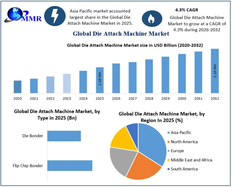
Long-Term Projection: The global market valuation is projected to steadily climb through 2032, expanding at an anticipated 4.3% CAGR as semiconductor packaging architectures shift away from traditional wire-bonding.
Type Dominance: Conventional Die Bonders held the major share of operational machine installations, backed by high-volume baseline discrete and analog chip processing lines.
Fastest-Growing Variant: Flip-Chip Bonders are experiencing the highest growth rate, accelerating at a 6.9% CAGR due to their superior capability in processing tight pitch, high-density 2.5D and 3D microelectronic configurations.
Technological Shift: Sintering and advanced eutectic techniques are rapidly taking market share from baseline epoxy methods, favored for high-temperature automotive electric vehicle (EV) inverters and power module setups.
Regional Superpower: The Asia-Pacific region controls the overwhelming majority of market share, hosting more than 60% of the world’s active OSAT production sites.
Why This Matters Now
The semiconductor fabrication and packaging ecosystem is hitting a critical technical wall. As traditional front-end transistor scaling slows down under physical limits, chip performance gains are migrating heavily to back-end advanced packaging innovation. Historically, packaging facilities relied on slower, single-die epoxy-dispense systems that tolerated loose alignment variations and manual setup checks. These legacy systems are increasingly unable to handle modern multi-die chiplets, high-frequency 5G components, and ultra-thin processors without high scrap rates and serious thermal bottlenecks.
Deploying highly automated, sub-micron accurate die attach machines addresses these precision and thermal bottlenecks directly. Modern flip-chip bonders and automated sintering equipment use vision-guided pattern recognition and dynamic force monitoring to position components with exact accuracy. This integration minimizes placement errors, eliminates voids in thermal interface materials, and ensures that complex multi-layer logic arrays achieve optimal throughput and thermal dissipation.
Market Overview
The global die attach machine market represents a foundational layer in the advanced electronics manufacturing supply chain, driving developments in consumer electronics, automotive computers, telecommunications hardware, and smart industrial sensors. Because modern electronic components require smaller footprints and higher I/O interconnect counts, advanced die attachment has become vital for building high-density memory arrays, CMOS image sensors, and high-frequency RF modules. The market’s steady path through 2032 outlines a global manufacturing migration toward high-speed, sub-micron precision assembly systems.
                        [WAFER EJECTOR NEEDLE TRACK]
                                     │
                                     ▼
                [VISION-GUIDED PATTERN RECOGNITION EYE]
               (Real-Time Sub-Micron Precision Alignment)
                                     │
                                     ▼
                [ULTRA-HIGH-SPEED PICK-AND-PLACE HEAD]
               (Dynamic Bond Force Compression Sensor)
                                     │
                                     ▼
                [THERMAL CONTROLLED FLUX/ADHESIVE BED]
              (Zero-Void Sintering or Epoxy Dispense)
                                     │
                                     ▼
                 [CONTINUOUS STRIP/SUBSTRATE DOWNLINE]
The expectations for back-end semiconductor equipment have shifted significantly under modern Industry 4.0 production guidelines. Modern packaging facilities require integrated assembly cells where the die attach system, automated fluid dispensers, and automated optical inspection (AOI) units communicate continuously on a unified digital framework to ensure high assembly yields.
Key Trends Driving Growth
The leading trend accelerating market expansion is the global transition toward chiplet-based designs and 2.5D/3D packaging architectures. High-performance applications like AI data centers, autonomous driving modules, and advanced graphics processors require several distinct dies to be placed side-by-side or stacked vertically on a single silicon interposer. Assembling these multi-die packages requires highly precise flip-chip and direct-die bonding tools equipped with advanced multi-axis voice coil actuators and real-time thermocompression modules capable of handling ultra-thin, fragile silicon dies.
Another primary driver is the widespread electrification and intelligence of modern vehicles. Electric vehicle power inverters and engine control units operate in harsh, high-temperature, high-vibration environments that can easily crack standard epoxy materials. To solve this, automotive component manufacturers are upgrading their assembly lines to specialized silver and copper sintering die attach machinery. These machines use high-pressure, thermal-assist systems to form incredibly stable, high-thermal-conductivity metal bonds that ensure long-term system reliability.
Additionally, the widespread deployment of Industrial IoT (IIoT) sensors and edge telemetry networks across smart factories has made real-time equipment diagnostic capability essential. Modern die attachment tools are built with continuous vacuum monitoring sensors in the pick nozzles, advanced thermal cameras on the bond heads, and predictive wear tracking for ejector needles. If an automated bonder detects an unexpected change in tool resistance, it flags the issue to technicians instantly, avoiding unexpected line shutdowns and preserving expensive production wafers.
Segment Insights
Die Bonder Machinery [Dominant Type]: This hardware segment held more than three-quarters of total market revenues, sustained by deep integration in consumer electronics, LED arrays, and analog power IC packaging lines.
Flip-Chip Bonders [Fastest-Growing Type]: This high-precision segment is expanding at an impressive 6.9% CAGR, driven by chipmakers building high-density, multi-pin processors for AI systems and high-speed data centers.
Epoxy Die Attach [Leading Technique]: This well-established method continues to lead total volume share, favored for its proven curing processes, low operational cost, and excellent compatibility with standard leadframe applications.
Sintering Systems: This advanced technique is seeing the highest investment growth among power electronics manufacturing firms, owing to the crucial demand for superior thermal management in EV electronics.
Assembly Technique Allocation Matrix
Choosing an optimal die attachment configuration involves balancing chemical properties, alignment tolerances, thermal profiles, and final application parameters.
| Technique Classification | Key Application Focus | Primary Structural Advantage | Core Engineering Focus |
| Epoxy Bond Systems | Consumer smartphones, standard LEDs, analog circuits | Low capital cost, highly flexible curing options | Focuses on high-speed dispensing valves and zero-stringing fluid control. |
| Soft Solder Solutions | High-power industrial diodes, baseline discrete devices | Reliable electrical conductivity, high stress relief | Demands specialized flux management and clean inert-gas environments. |
| Silver Sintering | EV power inverters, high-voltage industrial modules | Exceptional thermal conductivity, robust high-temp wear | Requires highly uniform bond force control to protect fragile dies under heat. |
| Eutectic Alloys (e.g., AuSn) | Optoelectronics, RF micro-parts, aerospace sensors | Instantaneous joint locking, zero-outgassing bonds | Demands strict, real-time closed-loop temperature profiles. |
Regional Growth Story
The Asia-Pacific region holds absolute dominance in the global die attach machine market, powered by massive semiconductor ecosystems in Taiwan, mainland China, South Korea, Japan, and Singapore. Because APAC hosts more than 60% of the world’s OSAT capacity, the region sees continuous, high-volume capital investments as these packaging firms upgrade to advanced multi-die bonding equipment to win high-tier foundry contracts.
Concurrently, North America is seeing an industrial resurgence, driven by significant investments in domestic semiconductor manufacturing, advanced defense microelectronics, and local aerospace engineering lines. Meanwhile, Europe maintains a specialized and highly innovative equipment hub, with packaging operations in Germany and France focusing tightly on developing high-reliability automotive components, industrial automation modules, and cutting-edge optical sensors.
Competitive Landscape
The competitive environment of the global die attach machine market is defined by rigorous sub-micron placement accuracy, robust mechanical design, and complete downline line automation. The top semiconductor equipment manufacturers have shifted from selling standalone machinery to supplying integrated packaging production systems. This development leaves smaller equipment builders at a disadvantage if they cannot deliver systems that smoothly connect wafer handling, precision dispensing, high-speed placement, and automated inspection under a single software interface.
Furthermore, engineering systems for sub-micron placement accuracy at high throughput rates serves as a primary area of competitive differentiation. Leading global equipment brands such as BE Semiconductor Industries N.V. (Besi), ASM Pacific Technology Limited (ASMPT), Kulicke & Soffa Industries, Inc., Fasford Technology Co. Limited, and Palomar Technologies maintain clear market leadership through continuous investments in multi-axis motion tracking systems, advanced bimetallic wear tooling, and integrated machine learning software. These capabilities allow advanced semiconductor factories to maximize production uptime, reduce material waste, and achieve repeatable quality across complex multi-die production batches.
Strategic Implications
For OSAT operational directors and semiconductor packaging executives, running legacy, manual, or low-accuracy die attach systems introduces a constant risk of high scrap rates and structural microchip failures. Relying on outdated bonding equipment results in slower changeover times, poor placement tolerances, and a complete lack of real-time bond force diagnostic metrics. These operational gaps increase technical strain on maintenance teams, raise per-unit production costs, and prevent a facility from bidding on high-precision advanced computing production orders.
For packaging line integration engineers, industrial distributors, and cleanroom automation developers, delivering open-architecture control systems and zero-void assembly modules is vital to winning long-term manufacturing contracts. As semiconductor assembly plants move toward fully automated, data-driven smart cleanrooms, equipment providers who supply isolated systems will be passed over during facility updates. Prioritizing SECS/GEM communication protocols, precise sub-micron vision feedback systems, and automated wear tracking is essential to maintaining market share.
Future Outlook
The future of the die attach machine market will be shaped by the deep integration of machine-learning-driven optical inspection, automated tool-wear optimization, and real-time hybrid bonding processes. As electronic designs continue to demand lower latency and smaller layouts, die attachment systems must function as highly precise, self-correcting assembly units. Future market leadership will belong to advanced systems that use machine learning to inspect bond fillets on the fly, automatically adjusting placement coordinates and thermal targets to keep production quality high without human intervention.
Ultimately, the market will split along clear technical capabilities: forward-looking chip packaging facilities that invest in intelligent, connected flip-chip and sintering lines will achieve higher production yields, lower waste, and process modern multi-die architectures easily, while assembly plants clinging to older mechanical configurations will face high material penalties and limited options in an increasingly precise semiconductor manufacturing industry.
Analyst Perspective
“The global die attach machine market has transitioned from basic chip placement to a high-precision, sub-micron automated discipline,” states an advanced semiconductor manufacturing analyst at Maximize Market Research. “As modern electronic components require higher placement accuracy and complex multi-die layouts, adopting smart flip-chip systems and advanced thermal sintering platforms gives packaging facilities the precise control and reliability needed to stay competitive.”
About Maximize Market Research
Maximize Market Research Pvt. Ltd. (MMR) is a global market research and consulting company that provides reliable, data-focused, and practical business insights. The firm serves a wide range of industries, including healthcare, pharmaceuticals, technology, automotive, electronics, chemicals, personal care, and consumer goods. Through market forecasts, competitive analysis, strategic consulting, and industry impact assessments, MMR helps organizations understand changing market conditions, identify growth opportunities, and make informed business decisions for long-term success.
2nd Floor, Navale IT Park Phase 3
Pune Banglore Highway, Narhe
Pune, Maharashtra 411041, India
+91 9607365656
sales@maximizemarketresearch.com
