Key Highlights
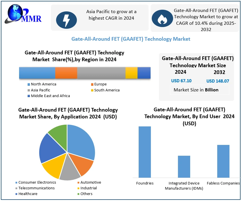
Global market valuation scales up from USD 67.10 billion in 2024 to USD 148.07 billion by 2032, achieving a 10.4 percent CAGR.
Nano-sheet GAAFET layouts dominate overall transistor type market share through superior electrostatic channel control and design scalability.
The consumer electronics sector serves as the leading application driver, sparked by high-volume demand for energy-efficient smartphone processors.
High manufacturing fabrication costs and sub-nanometer defect cleanroom complexities represent the primary market growth constraints.
Enhanced breakdown voltage parameters and minimized energy losses stabilize industrial long-term equipment capital deployment.
Why This Matters Now The semiconductor manufacturing sector is undergoing an abrupt process transition as traditional FinFET layouts hit physical scaling limits at the 3nm threshold. Legacy lithography lines and chemical etching processes are incapable of forming the 3D multi-layered horizontal nanowires or nanosheets required for sub-3nm nodes without inducing devastating quantum leakage. To maintain operational viability and prevent wafer yield failures, foundry operations must immediately transition to atomic-scale automation platforms, multi-chamber cluster tool control, and real-time robotic wafer handling.
This sweeping architecture shift demands that automation engineers and process control system integrators implement ultra-precise, closed-loop fluid delivery systems and advanced distributed control system architectures. Achieving sub-angstrom deposition uniformity requires the deployment of high-speed digital mass flow controllers and real-time gas-phase monitoring interfaces operating directly at the process edge. For technology buyers and institutional electronics investors, allocating capital to digital-twin-driven wafer fab equipment represents a fundamental requirement to secure profitable wafer margins.
Market Overview The global Gate-All-Around FET (GAAFET) Technology Market achieved a valuation of USD 67.10 billion in 2024 and is projected to reach USD 148.07 billion by 2032. This long-term technology lifecycle is expanding at a steady compound annual growth rate of 10.4 percent over the 2025–2032 forecast period. The underlying demand is closely tied to the massive infrastructure buildout of high-performance computing centers, advanced driver-assistance architectures, and 5G/6G telecommunication switches.
However, the fabrication of GAAFET components is severely constrained by exceptionally high initial research and development investments and complex manufacturing costs. Wafer processing facilities face steep financial exposure when engineering selective isotropic etching cycles that must carve away sacrificial silicon-germanium layers without altering the primary silicon nanosheets. Despite these complex front-end engineering barriers, the immense performance gains—including enhanced breakdown voltage metrics and elevated input impedance capabilities—sustain high-velocity tool procurement among leading global foundries.
Key Trends Driving Growth The convergence of atomic layer deposition (ALD) automation and machine learning process control is completely overhauling the productivity parameters of advanced cleanrooms. Semiconductor factories are replacing legacy batch chemical processing with automated single-wafer gas pulse systems that construct conformal gate oxides around all four sides of a suspended nanowire channel. Connecting these high-precision gas delivery systems into a plant-wide SCADA monitoring network allows process engineers to catch sub-nanometer deposition anomalies before they trigger wafer-level chip failures.
Simultaneously, the continuous requirement for minimized energy loss across battery-powered platforms is accelerating the deployment of nano-sheet transistor architecture. Manufacturing entities are shifting away from rigid planar structures to implement variable-width nanosheet configurations that maximize drive current while suppressing sub-threshold leakage currents. This structural flexibility allows automation designers to integrate sophisticated digital telemetry directly into the chip fabrication cycle, matching real-time tool performance metrics against a simulated digital twin to maximize factory asset efficiency.
Segment Insights
Nano-sheet GAAFETs (Dominant Segment — Transistor Type): Dominates total market share due to its superior electrostatic control capabilities, scaling advantages beyond FinFET limitations, and elevated drive current density. The business implication requires equipment vendors to supply highly integrated multi-station cluster tools equipped with ultra-precise chamber pressure regulation systems.
Consumer Electronics (Dominant Segment — Application): Leads overall application consumption profiles, propelled by the relentless consumer push for faster, smaller, and less power-demanding portable electronics. This high-volume demand forces foundries to invest heavily in automated robotic wafer sorting modules and automated optical inspection arrays to maximize cleanroom throughput.
Nanowire GAAFETs: Capturing key research and specialized product spaces where extreme sub-nanometer channel confinement and low parasitic capacitance profiles are required. This micro-scale application segment drives tool builders to engineer high-vacuum plasma chambers that utilize precise radio-frequency generator controllers to stabilize atomic-level etching paths.
Regional Growth Story The Asia-Pacific region holds the highest revenue share in the global landscape, sustained by the concentration of world-scale mega-foundries across Taiwan, South Korea, Japan, and mainland China. Regional semiconductor manufacturers are leading the global capital expenditure cycle, heavily deploying advanced extreme ultraviolet (EUV) lithography setups and automated manufacturing execution systems. This high concentration of wafer manufacturing infrastructure turns the region into the primary deployment epicenter for next-generation robotic wafer transport networks and predictive fab maintenance technologies.
North America and Europe continue to expand their market footprint through focused regional supply chain resilience programs and state-backed manufacturing funding. The United States and Germany are seeing substantial capital investments aimed at building localized sub-3nm logic fabs equipped with modern distributed control networks and advanced industrial IoT tracking layers. These mature regions emphasize deep process automation and advanced industrial cybersecurity frameworks to protect highly sensitive chip design and proprietary etching recipe profiles from unauthorized data extraction.
Competitive Landscape The competitive environment within the global GAAFET technology market features leading electronics and automation entities, including Infineon Technologies AG, Fairchild Semiconductor, Renesas Electronics Corporation, Digi-Key Electronics, Toshiba Corporation, IXYS Corporation, Power Integration, STMicroelectronics, NXP Semiconductors, and ABB Group. These tier-one suppliers are actively transitioning their internal asset strategies to provide fully automated, software-driven power and signal components. This shift alters market positioning, forcing traditional component providers to build deep software stacks and advanced telemetry loops around their solid-state hardware.
To secure durable market leadership, dominant semiconductor manufacturers are entering into long-term strategic equipment supply agreements with premium automation system builders. These partnerships ensure that newly built wafer lines feature native integration between atomic-level process tools and enterprise-level manufacturing execution layers. Semiconductor entities that rely on fragmented, older-generation process control interfaces will face escalating production costs and rapid commercial marginalization as the industry standardizes on fully automated sub-3nm nodes.
Recent Developments
Foundry operators have successfully integrated advanced high-speed digital mass flow controllers into ALD chambers to achieve angstrom-level precision on all four sides of the channel gate layer.
Advanced testing facilities are deploying machine-learning optical inspection tools to identify sub-nanometer lattice defects and structural dislocations on completed GAAFET wafer surfaces.
Equipment manufacturers have engineered new selective dry chemical etching systems that use precision thermal gas controls to carefully remove sacrificial silicon-germanium segments without damaging adjacent layers.
System integrators are rolling out automated factory execution updates that synchronize the movement of front-opening unified pods (FOUPs) with real-time chamber availability data to maximize tool utilization.
Security providers are installing hardware-based cryptographic root-of-trust modules inside semiconductor factory networks to secure high-value process recipes from edge-level operational technology vulnerabilities.
Strategic Implications For semiconductor executives and plant operations leaders, the shift to GAAFET architectures requires a complete reassessment of factory floor asset coordination. Replacing linear batch lines with fully automated, modular cluster tool systems allows foundries to run diverse etching and deposition cycles within a single, completely enclosed vacuum environment. This process centralization eliminates the risk of airborne molecular contamination during wafer transfers and drastically reduces the non-productive time associated with inter-tool transport.
Automation engineers must prioritize the clean integration of field instrumentation devices and high-vacuum gauge arrays with upper-tier data collection layers. Building highly responsive, low-latency communication paths ensures that chamber temperatures, gas ratios, and plasma density levels are constantly validated against exact recipe setpoints. This intense degree of system interaction requires robust industrial cybersecurity architectures to protect the plant floor from malicious network injections that could destroy entire multi-million dollar wafer lots.
Future Outlook The next stage of evolution for the advanced semiconductor market will center on the realization of autonomous, self-correcting fabrication environments. Production equipment will feature embedded cognitive control layers capable of modifying lithography focus offsets and chemical exposure times dynamically based on upstream inspection data. As international environmental oversight focuses heavily on reducing fluorinated gas consumption, utilizing automated closed-loop chemical capture systems will be vital to securing long-term corporate regulatory compliance.
The division between future industry leaders and laggards will depend entirely on the speed at which organizations implement comprehensive atomic process automation technologies. Industrial organizations that quickly incorporate modern software execution layers, multi-chamber robotic handling systems, and real-time edge telemetry will capture minimized tool downtime, exceptional chip yields, and accelerated technology node rollouts. Conversely, slow-moving device manufacturers relying on unmonitored legacy platforms will face unsustainable yield drops, escalating wafer rejections, and commercial extinction.
Analyst Perspective
“The transition to Gate-All-Around FET architectures represents a fundamental process control milestone in semiconductor history,” explains Gaurav Deshmukh, Lead Analyst at Maximize Market Research. “We have exited the era of macroscopic mechanical adjustments, meaning that sub-3nm chip yield viability now depends on atomic-scale automation and synchronized cluster chamber orchestration. Foundries that rapidly implement advanced closed-loop gas delivery systems and real-time machine-learning inspection layers will control the future of high-performance computing, while legacy operators sticking to unmonitored FinFET methods will find their operations commercially non-viable.”
About Maximize Market Research
Maximize Market Research Pvt. Ltd. (MMR) is a global market research and consulting company that provides reliable, data-focused, and practical business insights. The firm serves a wide range of industries, including healthcare, pharmaceuticals, technology, automotive, electronics, chemicals, personal care, and consumer goods. Through market forecasts, competitive analysis, strategic consulting, and industry impact assessments, MMR helps organizations understand changing market conditions, identify growth opportunities, and make informed business decisions for long-term success.
2nd Floor, Navale IT Park Phase 3
Pune Banglore Highway, Narhe
Pune, Maharashtra 411041, India
+91 9607365656
sales@maximizemarketresearch.com
